Reduce Scrapping and Smelting, Promote Component Reuse > Unpowered, Hand Tools
> Metalworking Tools
> Cook County
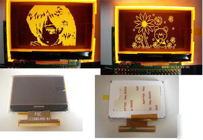
> 128*64 dot lcd moulde screen about 55* 40 mm orange
128*64 dot lcd moulde screen about 55* 40 mm orange
128*64 dot lcd moulde orange back light screen
128 * 64 lcd moulde dual back light orange selectable in program control st765s cog style
moudle size not including the lines is about 55* 40 mm
st765s can select parrallel or serial comunication
work voltage is about 3.3 volts dcd
no need negative voltage only need connect capcitor
orange back light is 3.3 volts dc .
look from front side the left first pin is 1 pin:
4 C86 6800 or 8080 interface H,6800 L,8080
// void LCD_DataWrite(unsigned int Data)
// write one byte to LCD display RAM
void LCD_DataWrite(unsigned char Dat)//,_Fill_Dot_LCD
if((Dat&0x80) = 0) LCD_SDI = 0;
// void LCD_RegWrite(unsigned char Command)
// write control byte LCD control resister
void LCD_RegWrite(unsigned char Command)
if((Command&0x80) = 0) LCD_SDI = 0;
// void LCD_Fill(unsigned int Data)
void LCD_Fill(unsigned char Data)
for(i=0;i<=uiTemp;i++) // fill ininitiallize data to LCD
//some ininitiallize data not all
//initiallize port connect to lcd moudle if necessary
LCD_RegWrite(M_LCD_ON); //LCD On
LCD_RegWrite(M_LCD_POWER_ALL); //set control model
LCD_RegWrite(M_LCD_ELE_VOL); //set light weet to stronge model
LCD_RegWrite(0x1f); //data instrument 0x0000~0x003f
LCD_RegWrite(M_LCD_VDD_SET); //V5 voltage resister adjust
LCD_RegWrite(M_LCD_VDD); //LCD voltage slant for V3 selected
LCD_RegWrite(M_LCD_COM_REV); //Com scan model
LCD_RegWrite(M_LCD_SEG_NOR); //Segment direction
LCD_RegWrite(M_LCD_ALL_LOW); //all screen light/gray down
LCD_RegWrite(M_LCD_ALL_NOR); //forward dicrection
LCD_RegWrite(M_LCD_STATIC_OFF); //close state display
LCD_RegWrite(0x00); //data instruntion
LCD_RegWrite(M_LCD_BEGIN_LINE); //set the RAM for starting line
the following is copied from st765s ic datasheet. you can google in google.
65 x 132 Dot Matrix LCD Controller/Driver
?? Direct display of RAM data through the display data
?? RAM capacity : 65 x 132 = 8580 bits
?? Display duty selectable by select pin
1/65 duty : 65 common x 132 segment
1/49 duty : 49 common x 132 segment
1/33 duty : 33 common x 132 segment
1/55 duty : 55 common x 132 segment
1/53 duty : 53 common x 132 segment
?? High-speed 8-bit MPU interface (The chip can be
connected directly to the both the 80x86 series MPUs
/Serial interfaces are supported.
Display data Read/Write, display ON/OFF, Normal/
Reverse display mode, page address set, display start
line set, column address set, status read, display all
points ON/OFF, LCD bias set, electronic volume,
read/modify/write, segment driver direction selects,
power saver, static indicator, common output status
select, V5 voltage regulation internal resistor ratio set.
?? Static drive circuit equipped internally for indicators.
(1 system, with variable flashing speed.)
?? Low-power liquid crystal display power supply circuit
Booster circuit (with Boost ratios of 2X/3X/4X/5X/6X
, where the step-up voltage reference power
supply can be input externally).
High-accuracy voltage adjustment circuit (Thermal
gradient 0.05%/ C ) V5 voltage regulator resistors
equipped internally, V1 to V4 voltage divider resistors
equipped internally, electronic volume function
equipped internally, voltage follower.
?? CR oscillator circuit equipped internally (external
?? Extremely low power consumption Operating power
when the built-in power supply is used (an example)
60uA (VDD VSS = VDD VSS2 =3.0 V, Quad voltage,
Conditions: When displays pattern OFF and the
?? Power supply operate on the low 1.8 voltage
VDD VSS = 1.8V to 3.3 V (+10% Range)
Boost reference voltage: VDD VSS2 = 1.8V to 3.3V
Booster maximum voltage limited
Liquid crystal drive power supply:
?? Wide range of operating temperatures: 40 to 85 C
?? These chips not designed for resistance to light or
The ST7565S is a single-chip dot matrix LCD driver that can
be connected directly to a microprocessor bus. 8-bit parallel
or serial display data sent from the microprocessor is stored
in the internal display data RAM and the chip generates a
LCD drive signal independent of the microprocessor.
Because the chips in the ST7565S contain 65x132 bits of
display data RAM and there is a 1-to-1 correspondence
between the LCD panel pixels and the internal RAM bits,
these chips enable displays with a high degree of freedom.
The ST7565S chips contain 65 common output circuits and
132 segment output circuits, so that a single chip can drive a
65x132 dot display (capable of displaying 8 columnsx4 rows
Moreover, the capacity of the display can be extended
through the use of master/slave structures between chips.
The chips are able to minimize power consumption
because no external operating clock is necessary for the
display data RAM read/write operation. Furthermore,
because each chip is equipped internally with a low-power
LCD driver power supply, resistors for LCD driver power
voltage adjustment and a display clock CR oscillator circuit,
the ST7565S can be used to create the lowest power display
system with the fewest components for high-performance
PART NO. VRS temperature gradient VRS range
ST7565S -0.05%/ C -2.1V 0.03V
Bump Size: PAD No. 001?012 40 m x 90 m
?? VOUT maximum -13V (+10% Range)
?? ST7565S Temperature gradient = -0.05%/ C
?? Logic power supply VDD VSS = 1.8V to 3.3 V (+10% Range)
?? Add new booster ratio 5 times and 6 times
?? Use select pin to define display duty as following table
Pad Center Coordinates (1/65 Duty)
Pad Center Coordinates (1/49 Duty)
Pad Center Coordinates (1/33 Duty)
Pad Center Coordinates (1/55 Duty)
Pad Center Coordinates (1/53 Duty)
MPU INTERFACE ( Parallel and Serial )
Status Command decoder Bus holder
Display timing generator circuit circuit
Pin Name I/O Function No. of Pins
Supply Shared with the MPU power supply terminal Vcc. 13
Supply This is a 0V terminal connected to the system GND. 10
This is the reference power supply for the step-up voltage circuit for the
This is the internal-output VREG power supply for the LCD power supply
This is a multi-level power supply for the liquid crystal drive. The voltage Supply
applied is determined by the liquid crystal cell, and is changed through the use of
a resistive voltage divided or through changing the impedance using an op. amp.
Voltage levels are determined based on VDD, and must maintain the relative
VDD (= V0) V1 V2 V3 V4 V5
When the power supply turns ON, the internal power supply circuits produce the
V1 to V4 voltages shown below. The voltage settings are selected using the LCD
1/65 DUTY 1/49 DUTY 1/33 DUTY 1/55 DUTY 1/53 DUTY
CAP1+ O DC/DC voltage converter. Connect a capacitor between this terminal and
CAP1 O DC/DC voltage converter. Connect a capacitor between this terminal and
CAP2+ O DC/DC voltage converter. Connect a capacitor between this terminal and
CAP2 O DC/DC voltage converter. Connect a capacitor between this terminal and
CAP3 O DC/DC voltage converter. Connect a capacitor between this terminal and
CAP4 O DC/DC voltage converter. Connect a capacitor between this terminal and
CAP5 O DC/DC voltage converter. Connect a capacitor between this terminal and
VOUT O DC/DC voltage converter. Connect a capacitor between this terminal and
Output voltage regulator terminal. Provides the voltage between VDD and
V5 through a resistive voltage divider.
IRS = L : the V5 voltage regulator internal resistors are not used .
IRS = H : the V5 voltage regulator internal resistors are used .
This is an 8-bit bi-directional data bus that connects to an 8-bit or 16-bit
When the serial interface is selected (P/S = L ) :
D7 : serial data input (SI) ; D6 : the serial clock input (SCL).
D0 to D5 are set to high impedance.
When the chip select is not active, D0 to D7 are set to high impedance.
This is connect to the least significant bit of the normal MPU address bus,
and it determines whether the data bits are data or a command.
A0 = H : Indicates that D0 to D7 are display data.
A0 = L : Indicates that D0 to D7 are control data.
When /RES is set to L, the settings are initialized.
The reset operation is performed by the /RES signal level.
This is the chip select signal. When /CS1 = L and CS2 = H, then the
chip select becomes active, and data/command I/O is enabled.
? When connected to an 8080 MPU, this is active LOW.
(E) This pin is connected to the /RD signal of the 8080 MPU, and the
ST7565S series data bus is in an output status when this signal is L .
? When connected to a 6800 Series MPU, this is active HIGH.
This is the 6800 Series MPU enable clock input terminal.
(R/W) This terminal connects to the 8080 MPU /WR signal. The signals on
the data bus are latched at the rising edge of the /WR signal.
? When connected to a 6800 Series MPU:
This is the read/write control signal input terminal.
This is the MPU interface switch terminal.
C86 = H : 6800 Series MPU interface.
C86 = L : 8080 MPU interface.
This is the parallel data input/serial data input switch terminal.
P/S = H : Parallel data input.
The following applies depending on the P/S status:
When P/S = L , D0 to D5 fixed H .
/RD (E) and /WR (R/W) are fixed to either H or L .
With serial data input, It is impossible read data from RAM .
P/S Data/Command Data Read/Write Serial Clock
L A0 SI (D7) Write only SCL (D6)
Terminal to select whether or enable or disable the display clock internal
CLS = H : used Internal oscillator circuit .
CLS = L : used external clock input .(internal oscillator is disable)
When CLS = L , input the display clock through the CL terminal.
This terminal selects the master/slave operation for the ST7565S Series chips.
Master operation outputs the timing signals that are required for the LCD display, while
slave operation input the timing signals required for the liquid crystal display,
Synchronizing the liquid crystal display system.
This is the display clock input terminal
The following is true depending on the M/S and CLS status.
FR O This is the liquid crystal alternating current signal terminal. 1
/DOF O This is the LCD blanking control terminal. 1
This is the output terminal for the static drive.
This terminal is only enabled when the static indicator display is ON
and is used in conjunction with the FR terminal.
This terminal selects the resistors for the V5 voltage level adjustment.
IRS = H : Use the internal resistors
IRS = L : Do not use the internal resistors. The V5 voltage level is
regulated by an external resistive voltage divider attached to the VR terminal
This is the power control terminal for the power supply circuit for liquid crystal
These pins are DUTY selection.
TEST0 ~ 5 I These are terminals for IC testing.
These are the LCD segment drive outputs. Through a combination of the
contents of the display RAM and with the FR signal, a single level is selected
Normal Display Reverse Display
Through a combination of the contents of the scan data and with the FR
signal, a single level is selected from VDD, V1, V4, and V5.
These are the COM output terminals for the indicator. Both terminals output
Leave these open if they are not used.
With the ST7565S chips, data transfers are done through an
8-bit parallel data bus (D7 to D0) or through a serial data
input (SI). Through selecting the P/ S terminal polarity to the
H or L it is possible to select either parallel
data input or serial data input as shown in Table 1.
P/S /CS1 CS2 A0 /RD /WR C86 D7 D6 D5~D0
H: Parallel Input /CS1 CS2 A0 /RD /WR C86 D7 D6 D5~D0
L: Serial Input /CS1 CS2 A0 SI SCL (HZ)
indicates fixed to either H or to L
When the parallel interface has been selected (P/S = H ),
then it is possible to connect directly to either an
8080-system MPU or a 6800 Series MPU (shown in Table 2)
by selecting the C86 terminal to either H or to L .
C86 (P/S=H) /CS1 CS2 A0 E(/RD) R/W(/WR
H: 6800 Series /CS1 CS2 A0 E R/W D7~D0
L: 8080 Series /CS1 CS2 A0 /RD /WR D7~D0
Moreover, data bus signals are recognized by a combination
of A0, /RD (E), /WR (R/W) signals, as shown in Table 3.
Shared 6800 Series 8080 Series
1 1 0 1 Reads the display data
1 0 1 0 Writes the display data
0 0 1 0 Write control data (command)
When the serial interface has been selected (P/S = L ) then
when the chip is in active state (/CS1 = L and CS2 = H )
the serial data input (SI) and the serial clock input (SCL) can
be received. The serial data is read from the serial data input
pin in the rising edge of the serial clocks D7, D6 through D0,
in this order. This data is converted to 8 bits parallel data in
the rising edge of the eighth serial clock for the processing.
The A0 input is used to determine whether or the serial data
input is display data or command data; when A0 = H , the
data is display data, and when A0 = L then the data is
command data. The A0 input is read and used for detection
every 8th rising edge of the serial clock after the chip
becomes active. Figure 1 is a serial interface signal chart.
1 2 3 4 5 6 7 8 9 10 11 12 13 14
D7 D6 D5 D4 D3 D2 D1 D0 D7 D6 D5 D4 D3 D2
* When the chip is not active, the shift registers and the counter are reset to their initial states.
* Reading is not possible while in serial interface mode.
* Caution is required on the SCL signal when it comes to line-end reflections and external noise. We recommend that
be rechecked on the actual equipment.
The ST7565S have two chip select terminals: /CS1 and CS2.
The MPU i n t e r f a c e o r the ser i a l int e r f ace i s
enabled only when /CS1 = L and CS2 = H .
When the chip select is inactive, D0 to D7 enter a high
impedance state, and the A0, /RD, and /WR inputs are
inactive. When the serial interface is selected, the shift
register and the counter are reset.
The Accessing the Display Data RAM and the Internal Registers
Data transfer at a higher speed is ensured since the MPU is
required to satisfy the cycle time (tCYC) requirement alone in
accessing the ST7565S. Wait time may not be considered.
And, in the ST7565S, each time data is sent from the MPU, a
type of pipeline process between LSIs is performed through
the bus holder attached to the internal data bus. Internal data
For example, when the MPU writes data to the display data
RAM, once the data is stored in the bus holder, then it is
written to the display data RAM before the next data write
cycle. Moreover, when the MPU reads the display data RAM,
the first data read cycle (dummy) stores the read data in the
bus holder, and then the data is read from the bus holder to
the system bus at the next data read cycle.
There is a certain restriction in the read sequence of the
display data RAM. Please be advised that data of the
specified address is not generated by the read instruction
issued immediately after the address setup. This data is
generated in data read of the second time. Thus, a dummy
read is required whenever the address setup
or write cycle operation is conducted.
When the busy flag is 1 it indicates that the ST7565S is
running internal processes, and at this time no command
aside from a status read will be received. The busy flag is
outputted to D7 pin with the read instruction. If the cycle time
(tCYC) is maintained, it is not necessary to check for this flag
before each command. This makes vast improvements in
MPU processing capabilities possible.
The display data RAM stores the dot data for the LCD. It has
a 65 (8 page x 8 bit +1) x 132 bit structure.
MPU corresponds to the LCD display common direction;
there are few constraints at the time of display data transfer
when multiple ST7565S are used, thus and display
structures can be created easily and with a high degree of
Moreover, reading from and writing to the display RAM from
the MPU side is performed through the I/O buffer, which is an
independent operation from signal reading for the liquid
crystal driver. Consequently, even if the display data RAM is
accessed asynchronously during liquid crystal display, it will
not cause adverse effects on the display (such as flickering).
Page address of the display data RAM is specified through
the Page Address Set Command. The page address must be
specified again when changing pages to perform access.
Page address 8 (D3, D2, D1, D0 = 1, 0, 0, 0) is a special
RAM for icons, and only display data D0 is used.
The display data RAM column address is specified by the
Column Address Set command. The specified column
address is incremented (+1) with each display data
read/write command. This allows the MPU display data to be
accessed continuously. Moreover, the incrementing of
column addresses stops with 83H. Because the column
address is independent of the page address, when moving,
for example, from page 0 column 83H to page 1 column 00H,
it is necessary to respective both the page address and the
(segment driver direction select command) can be used to
column address and the segment output. Because of this,
the constraints on the IC layout when the LCD module is
0 (H) Column Address 83 (H)
83 (H) Column Address 0 (H)
The line address circuit, as shown in Table 4, specifies the
line address relating to the COM output when the contents of
the display data RAM are displayed. Using the display start
line address set command, what is normally the top line of
the display can be specified (this is the COM0 output when
the common output mode is normal, and the COM63 output
for ST7565S , the detail is shown page.11 The display area
is a 65 line area for the ST7565S.
If the line addresses are changed dynamically using the
display start line address set command, screen scrolling,
page swapping, etc. can be performed.
The Display Data Latch Circuit
The display data latch circuit is a latch that temporarily stores
the display data that is output to the liquid crystal
driver circuit from the display data RAM.
Because the display normal/reverse status, display ON/OFF
status, and display all points ON/OFF commands control
only the data within the latch, they do not change
the data within the display data RAM itself.
This is a CR-type oscillator that produces the display clock.
The oscillator circuit is only enabled when M/S= H and CLS
When CLS = L the oscillation stops, and the external
clock is input through the CL terminal.
Display Timing Generator Circuit
The display timing generator circuit generates the timing
signal to the line address circuit and the display data latch
circuit using the display clock. The display data is latched into
the display data latch circuit synchronized with the display
clock, and is output to the data driver output terminal.
Reading to the display data liquid crystal driver circuits is
completely independent of accesses to the display data RAM
by the MPU. Consequently, even if the display data RAM is
accessed asynchronously during liquid crystal display, there
i s a b s o l u t e l y n o a d v e r s e e f f e c t ( s u c h a s
Moreover, the display timing generator circuit generates the
common timing and the liquid crystal alternating current
signal (FR) from the display clock. It generates a drive wave
shown in Figure 5, for the liquid crystal drive circuit.
Two-frame alternating current drive waveform
64 65 1 2 3 4 5 6 60 61 62 63 64 65 1 2 3 4 5 6
The Common Output Status Select Circuit
In the ST7565S chips, the COM output scan direction can be
selected by the common output status select command.
(See Table 6.) Consequently, the constraints in IC layout at
the time of LCD module assembly can be minimized.
dir com[0:15] com[16:23] com[24:26] com[27:36] com[37:39] com[40:47] com[48:63] coms
0 com[0:23] reserve com[24:47] coms
1 com[47:24] reserve com[23:0] coms
0 com[0:15] reserve com[16:31] coms
1 com[31:16] reserve com[15:0] coms
0 com[0:26] reserve com[27:53] coms
1 com[53:27] reserve com[26:0] coms
0 com[0:25] reserve com[26:51] coms
1 com[51:26] reserve com[25:0] coms
These are a 187-channel that generates four voltage levels
for driving the LCD . The combination of the display data, the
COM scan signal, and the FR signal produces the liquid
Figure 6 shows examples of the SEG and COM output
The power supply circuits are low-power consumption power
supply circuits that generate the voltage levels required for
the LCD drivers. They are Booster circuits, voltage regulator
circuits, and voltage follower circuits. They are only enabled
in master operation. The power supply circuits can turn the
Booster circuits, the voltage regulator circuits, and the
voltage follower circuits ON or OFF independently through
the use of the Power Control Set command. Consequently, it
is possible to make an external power supply and the internal
power supply function somewhat in parallel. Table 7 shows
the Power Control Set Command 3-bit data control function,
and Table 8 shows reference combinations.
Voltage regulator circuit control bit (V/R circuit)
Voltage follower circuit control bit (V/F circuit)
The Control Details of Each Bit of the Power Control Set Command
Only the internal power supply is used 1 1 1 ON ON ON VSS2 Used
Only the voltage regulator circuit and the
voltage follower circuit are used
0 1 1 OFF ON ON VOUT, VSS2 Open
Only the V/F circuit is used 0 0 1 OFF OFF ON V5, VSS2 Open
Only the external power supply is used 0 0 0 OFF OFF OFF V1 to V5 Open
* The step-up system terminals refer CAP1+, CAP1 , CAP2+, CAP2 , and CAP3 .
* While other combinations, not shown above, are also possible, these combinations are not recommended
because they have no practical use.
Using the step-up voltage circuits equipped within the
ST7565S chips it is possible to product a 2X,3X,4X,5X or 6X
step-up of the VDD VSS2 voltage levels.
6X step-up: Connect capacitor C1 between CAP1+ and
CAP1 , between CAP2+ and CAP2 , between
CAP1+ and CAP3 , between CAP2+ and
CAP4 ,between CAP1+ and CAP5 , and
between VSS2 and VOUT, to produce a voltage
level in the negative direction at the VOUT
terminal that is 6 times the voltage level
5X step-up: Connect capacitor C1 between CAP1+ and
CAP4 ,and between VSS2 and VOUT, to
produce a voltage level in the negative direction
at the VOUT terminal that is 5 times the voltage
4X step-up: Connect capacitor C1 between CAP1+ and
CAP1+ and CAP3 , and between VSS2 and
VOUT, to produce a voltage level in the negative
direction at the VOUT terminal that is 4 times the
voltage level between VDD and VSS2.
3X step-up: Connect capacitor C1 between CAP1+ and CAP1 , between
CAP2+ and CAP2 and between VSS2 and VOUT, and short
between CAP3 and VOUT to produce voltages
terminal that is 3 times the voltage difference
2X step-up: Connect capacitor C1 between CAP1+ and
CAP1 , and between VSS2 and VOUT, leave
CAP2+ open, and short between CAP2 ,
CAP3 and VOUT to produce a voltage in the
negative direction at the VOUT terminal that Is
twice the voltage between VDD and VSS2.
4x step-up voltage circuit 3x step-up voltage circuit 2x step-up voltage circuit
* The VSS2 voltage range must be set so that the VOUT terminal voltage does not exceed the absolute maximum rated
The step-up voltage generated at VOUT outputs the LCD
driver voltage V5 through the voltage regulator circuit.
Because the ST7565S chips have an internal high-accuracy
fixed voltage power supply with a 64-level electronic volume
function and internal resistors for the V5 voltage regulator,
systems can be constructed without having to include
high-accuracy voltage regulator circuit components.
(VREG thermal gradients approximate -0.05%/ C)
(A) When the V5 Voltage Regulator Internal Resistors Are Used
Through the use of the V5 voltage regulator internal resistors
and the electronic volume function the liquid crystal power
supply voltage V5 can be controlled by commands alone
(without adding any external resistors), making it possible to
adjust the liquid crystal display brightness. The V5 voltage
can be calculated using equation A-1 over the range where
VEV(constant voltage supply+electronic volume)
VREG is the IC-internal fixed voltage supply, and its voltage at Ta = 25 C is as shown in Table 9.
Part no. Equipment Type Thermal Gradient VREG
ST7565S Internal Power Supply 0.05 %/ C 2.1V
is set to 1 level of 64 possible levels by the electronic volume function depending on the data set in the 6-bit
volume registers. Table 10 shows the value for depending on the electronic volume register settings.
Rb/Ra is the V5 voltage regulator internal resistor ratio, and can be set to 8 different levels through the V5
internal resistor ratio set command. The (1 + Rb/Ra) ratio assumes the values shown in Table 11 depending on the 3
settings in the V5 voltage regulator internal resistor ratio register.
V5 voltage regulator internal resistance ratio register value and (1 + Rb/Ra) ratio (Reference value)
Figures 9, 10 show V5 voltage measured by values of the internal resistance ratio resistor for V5 voltage
volume resister for each temperature grade model.
Ta = 25 C and booster off ,regulator,follower on VSS=-3V
Figure 9 : (1) For ST7565S the Thermal Gradient = -0.05%/ C
The V5 voltage as a function of the V5 voltage regulator internal resistor ratio register and the electronic volume
Setup example: When selecting Ta = 25 C and V5 = 7V for an ST7565S on which Temperature gradient = 0.05%/ C.
Using Figure 9 and the equation A-1, the following setup is enabled.
At this time, the variable range and the notch width of the V5 voltage is, as shown Table 13, as dependent on the
Contents D5 D4 R De3g i sDt2e r D1 D0
8.4 (63 levels) 7.0 (central value) 5.1 (0 level) [V]
(B) When an External Resistance is Used (The V5 Voltage Regulator Internal Resistors Are Not Used) (1)
The liquid crystal power supply voltage V5 can also be set
without using the V5 voltage regulator internal resistors (IRS
terminal = L ) by adding resistors Ra and Rb between VDD
and VR, and between VR and V5, respectively. When this is
done, the use of the electronic volume function makes it
possible to adjust the brightness of the liquid crystal display
by controlling the liquid crystal power supply voltage V5
In the range where | V5 | < | VOUT |, the V5 voltage can be
calculated using equation B-1 based on the external
VEV(fixed voltage power supply+electronic volume)
Setup example: When selecting Ta = 25 C and V5 = 7 V for
ST7565S the temperature gradient = 0.05%/ C.
When the central value of the electron volume register is
(D5, D4, D3, D2, D1, D0) = (1, 0, 0, 0, 0, 0), then = 31 and
VREG = 2.1V so, according to equation B-1,
Moreover, when the value of the current running through
Consequently, by equations B-2 and B-3,
At this time, the V5 voltage variable range and notch
width, based on the electron volume function, is as
8.6 (63 levels) 7.0 (central value) 5.3 (0 level) [V]
(C) When External Resistors are Used (The V5 Voltage Regulator Internal Resistors Are Not Used) (2)
When the external resistor described above are used, adding
a variable resistor as well makes it possible to perform fine
adjustments on Ra and Rb , to set the liquid crystal drive
voltage V5. In this case, the use of the electronic volume
function makes it possible to control the liquid crystal power
supply voltage V5 by commands to adjust the liquid
In the range where | V5 | < | VOUT | the V5 voltage can be
calculated by equation C-1 below based on the R1 and R2
(variable resistor) and R3 settings, where R2 can
be subjected to fine adjustments ( R2).
Setup example: When selecting Ta = 25 C and V5 = 5 to 9
V (using R2) for an ST7565S the temperature gradient
When the central value for the electronic volume register is
set at (D5, D4, D3, D2, D1, D0) = (1, 0, 0, 0, 0, 0), then =
31 and VREG = 2.1 V so, according to equation C-1, when
R2 = 0 , in order to make V5 = 9 V,
When R2 = R2, in order to make V = 5 V,
When the current flowing VDD and V5 is set to 5 uA,
With this, according to equation C-2, C-3 and C-4,
The V5 voltage variable range and notch width based on the
electron volume function is as shown in Table 15.
8.7 (63 levels) 7.0 (central value) 5.3 (0 level) [V]
-40 C -20 C 0 C 25 C 50 C 85 C
* When the V5 voltage regulator internal resistors or the electronic volume function is used, it is necessary to at
voltage regulator circuit and the voltage follower circuit to an operating mode using the power control set
Moreover, it is necessary to provide a voltage from VOUT when the Booster circuit is OFF.
* The VR terminal is enabled only when the V5 voltage regulator internal resistors are not used (i.e. the IRS
When the V5 voltage regulator internal resistors are used (i.e. when the IRS terminal = H ), then the VR
* Because the input impedance of the VR terminal is high, it is necessary to take into consideration short leads,
The LCD Voltage Generator Circuit
The V5 voltage is produced by a resistive voltage divider
within the IC, and can be produced at the V1, V2, V3, and V4
voltage levels required for liquid crystal driving. Moreover,
when the voltage follower changes the impedance, it
provides V1, V2, V3 and V4 to the liquid crystal drive circuit.
The power supply circuit equipped in the ST7565S chips has
very low power consumption (normal mode: HPM = H ).
However, for LCDs or panels with large loads, this low-power
power supply may cause display quality to degrade. When
this occurs, setting the HPM terminal to L (high power mode)
can improve the quality of the display. We recommend that
the display be checked on actual equipment to determine
whether or not to use this mode. Moreover, if the
improvement to the display is inadequate even after high
power mode has been set, then it is necessary to add a liquid
c r y s t a l d r i v e p o w e r s u p p l y
The Internal Power Supply Shutdown Command Sequence
The sequence shown in Figure 13 is recommended for
shutting down the internal power supply, first placing the
power supply in power saver mode and then turning
Sequence Details Command address
(Command, status) D7 D6 D5 D4 D3 D2 D1 D0
Step1 Display OFF 1 0 1 0 1 1 1 0 Power saver
Step2 Display all points ON 1 0 1 0 0 1 0 1 commands
End Internal power supply OFF (compound)
The temperature grade of the Internal Power Supply for ST7565S (-0.05%/ C) :
Figure 15 shows reference circuit examples.
1. When used all of the step-up circuit, voltage regulating circuit and V/F circuit
(1) When the voltage regulator internal resistor
(Example where VSS2 = VSS, with 4x step-up)
(2) When the voltage regulator internal resistor
2. When the voltage regulator circuit and V/F circuit alone are used
(1) When the V5 voltage regulator internal resistor
(2) When the V5 voltage regulator internal resistor
3. When the V/F circuit alone is used 4. When the built-in power is not used
5. When the built-in power circuit is used to drive a liquid
crystal panel heavily loaded with AC or DC, it is
recommended to connect an external resistor to stabilize
potentials of V1, V2, V3 and V4 which are output from the
Examples of shared reference settings When V5 can vary
Reference set value R4: 100K ~ 1M It is recommended
to set an optimum resistance value R4 taking the liquid
crystal display and the drive waveform.
* 1. Because the VR terminal input impedance is high, use short leads and shielded lines.
* 2. C1 and C2 are determined by the size of the LCD being driven. Select a value that will stabilize the liquid
Example of the Process by which to Determine the Settings:
? Turn the voltage regulator circuit and voltage follower circuit ON and supply a voltage to VOUT from the outside.
? Determine C2 by displaying an LCD pattern with a heavy load (such as horizontal stripes) and selecting a C2 that
liquid crystal drive voltages (V1 to V5). Note that all C2 capacitors must have the same capacitance value.
? Next turn all the power supplies ON and determine C1.
C1 and C2 are determined by the size of
When the /RES input comes to the L level, these LSIs
return to the default state. Their default states are as follows:
3. ADC select: Normal (ADC command D0 = L )
4. Power control register: (D2, D1, D0) = (0, 0, 0)
5. Serial interface internal register data clear
6. LCD power supply bias rate:
1/49,1/55,1/53 DUTY = 1/8 bias
7. All-indicator lamps-on OFF (All-indicator lamps ON/OFF
9. V5 voltage regulator internal resistors Ra and Rb
10. Output conditions of SEG and COM terminals
12. Static indicator OFF Static indicator register : (D1, D2) =
13. Display start line set to first line
14. Column address set to Address 0
15. Page address set to Page 0
16. Common output status normal
17. V5 voltage regulator internal resistor ratio set mode clear
18. Electronic volume register set mode clear Electronic
(D5, D4, D3, D2, D1, D0) = (1, 0. 0, 0, 0,0)
On the other hand, when the reset command is used, the
above default settings from 11 to 19 are only executed.
When the power is turned on, the IC internal state becomes
unstable, and it is necessary to initialize it using the /RES
terminal. After the initialization, each input terminal should
Moreover, when the control signal from the MPU is in the
high impedance, an over current may flow to the IC. After
applying a current, it is necessary to take proper measures to
prevent the input terminal from getting into the high
If the internal liquid crystal power supply circuit is not used on
ST7565S,it is necessary that /RES is H when the external
liquid crystal power supply is turned on. This IC has the
function to discharge V5 when /RES is L, and the external
power supply short-circuits to VDD when /RES is L.
While /RES is L, the oscillator and the display timing
generator stop, and the CL, FR, FRS and /DOF terminals are
fixed to H. The terminals D0 to D7 are not affected. The
VDD level is output from the SEG and COM output terminals.
This means that an internal resistor is connected between
When the internal liquid crystal power supply circuit is not
used on other models of ST7565S series, it is necessary that
/RES is L when the external liquid crystal power supply is
While /RES is L, the oscillator works but the display timing
generator stops, and the CL, FR, FRS and /DOF terminals
are fixed to H. The terminals D0 to D7 are not affected.
The ST7565S identify the data bus signals by a combination of A0, /RD (E), /WR(R/W) signals. Command interpretation
execution does not depend on the external clock, but rather is performed through internal timing only, and
thus the processing is fast enough that normally a busy check is not required.
In the 8080 MPU interface, commands are launched by inputting a low pulse to the RD terminal for reading, and
pulse to the /WR terminal for writing. In the 6800 Series MPU interface, the interface is placed in a read mode
is input to the R/W terminal and placed in a write mode when a L signal is input to the R/W terminal and then
launched by inputting a high pulse to the E terminal. Consequently, the 6800 Series MPU interface is different than
Series MPU interface in that in the explanation of commands and the display commands the status read and display
/RD (E) becomes 1(H) . In the explanations below the commands are explained using the 8080 Series MPU interface
When the serial interface is selected, the data is input in sequence starting with D7.
This command turns the display ON and OFF.
When the display OFF command is executed when in the display all points ON mode, power saver mode is entered. See
section on the power saver for details.
This command is used to specify the display start line address of the display data RAM shown in Figure 4. For
see the explanation of this function in The Line Address Circuit .
This command specifies the page address corresponding to the low address when the MPU accesses the display data RAM
(see Figure 4). Specifying the page address and column address enables to access a desired bit of the display data
Changing the page address does not accompany a change in the status display.
This command specifies the column address of the display data RAM shown in Figure 4. The column address is split
sections (the higher 4 bits and the lower 4 bits) when it is set (fundamentally, set continuously). Each time the
is accessed, the column address automatically increments (+1), making it possible for the MPU to continuously read
to the display data. The column address increment is topped at 83H. This does not change the page address
the function explanation in The Column Address Circuit, for details.
D7 D6 D5 D4 D3 D2 D1 D0 A7 A6 A5 A4 A3 A2 A1 A0
0 0 0 1 A7 A6 A5 A4 0 0 0 0 0 0 0 0
0 0 1 BUSY ADC ON/OFF RESET 0 0 0 0
BUSY = 1: it indicates that either processing is occurring internally or a reset condition is in process.
BUSY = 0: A new command can be accepted . if the cycle time can be satisfied, there is no need to check
0: Normal (column address n ? SEG n)
1: Reverse (column address 131-n ? SEG n)
(The ADC command switches the polarity.)
ON/OFF: indicates the display ON/OFF state.
(This display ON/OFF command switches the polarity.)
This indicates that the chip is in the process of initialization either because of a /RES signal or because of a
This command writes 8-bit data to the specified display data RAM address. Since the column address is automatically
incremented by 1 after the write, the MPU can write the display data.
This command reads 8-bit data from the specified display data RAM address. Since the column address is
incremented by 1 after the read, the CPU can continuously read multiple-word data. One dummy read is required
after the column address has been set. See the function explanation in Display Data RAM for the explanation of
internal registers. When the serial interface is used, reading of the display data becomes unavailable.
ADC Select (Segment Driver Direction Select)
This command can reverse the correspondence between the display RAM data column address and the segment driver
Thus, sequence of the segment driver output pins may be reversed by the command. See the column address circuit
1 20) for the detail. Increment of the column address (by 1 ) accompanying the reading or writing the display
according to the column address indicated in Figure 4.
This command can reverse the lit and unlit display without overwriting the contents of the display data RAM. When
the display data RAM contents are maintained.
This command makes it possible to force all display points ON regardless of the content of the display data RAM.
of the display data RAM are maintained when this is done. This command takes priority over the display
When the display is in an OFF mode, executing the display all points ON command will place the display in power
For details, see the Power Save section.
This command selects the voltage bias ratio required for the liquid crystal display.
D7 D6 D5 D4 D3 D2 D1 D0 1/65duty 1/49duty 1/33duty 1/55duty 1/53duty
1/9 bias 1/8 bias 1/6 bias 1/8 bias 1/8 bias
1 1/7 bias 1/6 bias 1/5 bias 1/6 bias 1/6 bias
This command is used paired with the END command. Once this command has been input, the display data read
does not change the column address, but only the display data write command increments (+1) the column address.
is maintained until the END command is input. When the END command is input, the column address returns to the
was at when the read/modify/write command was entered. This function makes it possible to reduce the load on the
there are repeating data changes in a specified display region, such as when there is a blanking cursor.
* Even in read/modify/write mode, other commands aside from display data read/write commands can also be used.
Figure 24 Command Sequence For read modify write
This command releases the read/modify/write mode, and returns the column address to the address it was at when the
This command initializes the display start line, the column address, the page address, the common output mode, the
regulator internal resistor ratio, the electronic volume, and the static indicator are reset, and the
test mode are released. There is no impact on the display data RAM. See the function explanation in Reset for
The reset operation is performed after the reset command is entered.
The initialization when the power supply is applied must be done through applying a reset signal to the /RES
command must not be used instead.
This command can select the scan direction of the COM output terminal. For details, see the function explanation in
Common Output Mode Select Circuit.
This command sets the power supply circuit functions. See the function explanation in The Power Supply Circuit,
Voltage regulator circuit: OFF
0 1 0 Voltage regulator circuit: ON
V5 Voltage Regulator Internal Resistor Ratio Set
This command sets the V5 voltage regulator internal resistor ratio. For details, see the function explanation is
Regulator circuit " and table 11 .
The Electronic Volume (Double Byte Command)
This command makes it possible to adjust the brightness of the liquid crystal display by controlling the LCD drive
through the output from the voltage regulator circuits of the internal liquid crystal power supply. This command is
command used as a pair with the electronic volume mode set command and the electronic volume register set
command, and both commands must be issued one after the other.
The Electronic Volume Mode Set
When this command is input, the electronic volume register set command becomes enabled. Once the electronic volume
has been set, no other command except for the electronic volume register command can be used. Once the electronic
volume register set command has been used to set data into the register, then the electronic volume mode is
Electronic Volume Register Set
By using this command to set six bits of data to the electronic volume register, the liquid crystal drive voltage
When this command is input, the electronic volume mode is released after the electronic volume register has been
When the electronic volume function is not used, set this to (1, 0, 0, 0, 0, 0)
The Electronic Volume Register Set Sequence
Static Indicator (Double Byte Command)
This command controls the static drive system indicator display. The static indicator display is controlled by this
and is independent of other display control commands.
This is used when one of the static indicator liquid crystal drive electrodes is connected to the FR terminal, and
connected to the FRS terminal. A different pattern is recommended for the static indicator electrodes than for the
electrodes. If the pattern is too close, it can result in deterioration of the liquid crystal and of the
The static indicator ON command is a double byte command paired with the static indicator register set command, and
one must execute one after the other. (The static indicator OFF command is a single byte command.)
When the static indicator ON command is entered, the static indicator register set command is enabled. Once the
indicator ON command has been entered, no other command aside from the static indicator register set command can be
This mode is cleared when data is set in the register by the static indicator register set command.
This command sets two bits of data into the static indicator register, and is used to set the static indicator into
ON (blinking at approximately one second intervals)
ON (blinking at approximately 0.5 second intervals)
Static Indicator Register Set Sequence
When the display all points ON is performed while the display is in the OFF mode, the power saver mode is entered,
greatly reducing power consumption.
The power saver mode has two different modes: the sleep mode and the standby mode. When the static indicator is
the sleep mode that is entered. When the static indicator is ON, it is the standby mode that is entered.
power saver mode was initiated, and the MPU is still able to access the display data RAM.
Refer to figure 28 for power save off sequence.
This stops all operations in the LCD display system, and as long as there are no accesses from the MPU, the
current is reduced to a value near the static current. The internal modes during sleep mode are as follows:
1. The oscillator circuit and the LCD power supply circuit are halted.
2. All liquid crystal drive circuits are halted, and the segment in common drive outputs output a VDD level.
The duty LCD display system operations are halted and only the static drive system for the indicator continues to
providing the minimum required consumption current for the static drive. The internal modes are in the following
1 The LCD power supply circuits are halted. The oscillator circuit continues to operate.
2 The duty drive system liquid crystal drive circuits are halted and the segment and common driver outputs output a
The static drive system does not operate.
When a reset command is performed while in standby mode, the system enters sleep mode.
* When an external power supply is used, it is recommended that the functions of the external power supply circuit
when the power saver mode is started. For example, when the various levels of liquid crystal drive voltage are
external resistive voltage dividers, it is recommended that a circuit be added in order to cut the electrical
through the resistive voltage divider circuit when the power saver mode is in effect. The ST7565S series chips have
crystal display blanking control terminal /DOF. This terminal enters an L state when the power saver mode is
Using the output of /DOF, it is possible to stop the function of an external power supply circuit.
* When the master is turned on, the oscillator circuit is operable immediately after the powering on.
The Booster Ratio (Double Byte Command)
This command makes it possible to select step-up ratio. It is used when the power control set have turn on the
circuit. This command is a two byte command used as a pair with the booster ratio select mode set command and the
ratio register set command, and both commands must be issued one after the other.
When this command is input, the Booster ratio register set command becomes enabled. Once the booster ratio select
been set, no other command except for the booster ratio register command can be used. Once the booster ratio
set command has been used to set data into the register, then the booster ratio select mode is released.
By using this command to set two bits of data to the booster ratio register,it can be select what kind of the
When this command is input, the booster ratio select mode is released after the booster ratio register has been
When the booster ratio select function is not used, set this to (0, 0) 2x,3x,4x step-up mode
The booster ratio Register Set Sequence
This is a command for IC chip testing. Please do not use it. If the test command is used by accident, it can be
applying a L signal to the /RES input by the reset command or by using an NOP.
Note: The ST7565S maintain their operating modes until something happens to change them. Consequently, excessive
external noise, etc., can change the internal modes of the ST7565S . Thus in the packaging and system design it is
necessary to suppress the noise or take measure to prevent the noise from influencing the chip. Moreover, it is
recommended that the operating modes be refreshed periodically to prevent the effects of unanticipated
Booster ratio select mode clear
Table 16: Table of ST7565S Commands (Note) *: disabled data
(1) Display ON/OFF 0 1 0 1 0 1 0 1 1 1 0
(2) Display start line set 0 1 0 0 1 Display start address Sets the display RAM display start
(3) Page address set 0 1 0 1 0 1 1 Page address Sets the display RAM page
Sets the most significant 4 bits of
the display RAM column address.
Sets the least significant 4 bits of
(5) Status read 0 0 1 Status 0 0 0 0 Reads the status data
(6) Display data write 1 1 0 Write data Writes to the display RAM
(7) Display data read 1 0 1 Read data Reads from the display RAM
(8) ADC select 0 1 0 1 0 1 0 0 0 0 0
(11) LCD bias set 0 1 0 1 0 1 0 0 0 1 0
Sets the LCD drive voltage bias
0: 1/9 bias, 1: 1/7 bias (ST7565S)
(12) Read/modify/write 0 1 0 1 1 1 0 0 0 0 0
(13) End 0 1 0 1 1 1 0 1 1 1 0 Clear read/modify/write
(14) Reset 0 1 0 1 1 1 0 0 0 1 0 Internal reset
mode select 0 1 0 1 1 0 0 0 * * *
Select COM output scan direction
(16) Power control set 0 1 0 0 0 1 0 1 Operating
(21) Power saver Display OFF and display all
(22) NOP 0 1 0 1 1 1 0 0 0 1 1 Command for non-operation
(23) Test 0 1 0 1 1 1 1 * * * * Command for IC test. Do not
Note: With this IC, when the power is applied, LCD driving non-selective potentials V2 and V3 (SEG pin) and V1 and
pin) are output through the LCD driving output pins SEG and COM. When electric charge is remaining in the smoothing
capacitor connecting between the LCD driving voltage output pins (V1 ~ V5) and the VDD pin, the picture on the
become totally dark instantaneously when the power is turned on. To avoid occurrence of such a failure, we
following flow when turning on the power.
1. When the built-in power is being used immediately after turning on the power:
* The target time of 5ms will result to vary depending on the panel characteristics and the capacitance of the
capacitor. Therefore, we suggest you to conduct an operation check using the actual equipment.
Notes: Refer to respective sections or paragraphs listed below.
*1: Description of functions; Resetting circuit
*2: Command description; LCD bias setting
*3: Command description; ADC selection
*4: Command description; Common output state selection
*5: Description of functions; Power circuit & Command description; Setting the built-in resistance radio for
Release the reset state. (/RES pin = H )
This concludes the initialization
Function setup by command input
(17) Setting the built-in resistance radio
for regulation of the V5 voltage *5
(18) Electronic volume control *6
(15) Common output state selection *4
Initialized state (Default) *1
reset state through setting the
turning on the power to setting
*6: Description of functions; Power circuit & Command description; Electronic volume control
*7: Description of functions; Power circuit & Command description; Power control setting
2. When the built-in power is not being used immediately after turning on the power:
*8: The power saver ON state can either be in sleep state or stand-by state.
Turn ON the VDD-VSS power keeping the
Function setup by command input (User
Command description; Power saver START (multiple commands)
*9: Command Description; Display start line set
*10: Command Description; Page address set
*11: Command Description; Column address set
*12: Command Description; Display data write
*13: Command Description; Display ON/OFF
Avoid displaying all the data at the data display start (when the display is ON) in white.
*14: The logic circuit of this IC s power supply VDD - VSS controls the driver of the LCD power supply VDD - V5.
power supply VDD - VSS is cut off when the LCD power supply VDD - V5 has still any residual voltage, the driver
(COM. SEG) may output any uncontrolled voltage. When turning off the power, observe the following basic
? After turning off the internal power supply, make sure that the potential V5 ~ V1 has become below the threshold
voltage of the LCD panel, and then turn off this IC s power supply (VDD - VSS). 6. Description of Function, 6.7
*15: After inputting the power save command, be sure to reset the function using the /RES terminal until the power
supply VDD - VSS is turned off. 7. Command Description (20) Power Save
*16: After inputting the power save command, do not reset the function using the /RES terminal until the power
VDD - VSS is turned off. 7. Command Description (20) Power Save
Optional status Set the time (tL) from reset
active to turning off the VDD -
longer than the time (tH) when
the LCD panel. For tH, refer to
It is recommended to turn on the refresh sequence regularly at a specified interval.
Precautions on Turning off the power
1) Power Save (The LCD powers (VDD - V5) are off.) Reset input Power (VDD - VSS) OFF
? When tL < tH, an irregular display may occur.
Set tL on the MPU according to the software. tH is determined according to the external capacity C2 (smoothing
capacity of V5 ~ V1) and the driver s discharging capacity.
About 1V:below Vth of the LCD Panel
Since the power (VDD-VSS) is cut off,the
Set all commands to the ready state
2) Reset (The LCD powers (VDD - VSS) are off.) Power (VDD - VSS) OFF
For tL, make the power (VDD - VSS) falling characteristics longer or consider any other method. tH is
determined according to the external capacity C2 (smoothing capacity of V5 to V1) and the driver s discharging
V5 voltage falling (discharge) time (tH) after the process of operation power save reset.
V5 voltage falling (discharge) time (tH) after the process of operation reset.
V5 voltage falling time (mSec)
Unless otherwise noted, VSS = 0V
Parameter Symbol Conditions Unit
Power Supply Voltage VDD 0.3 ~ +5.0 V
Power supply voltage (VDD standard) VSS2 4.0 ~ -1.8 V
Power supply voltage (VDD standard) V5, VOUT 16.0 ~ +0.3 V
Power supply voltage (VDD standard) V1, V2, V3, V4 V5 to +0.3 V
Input voltage VIN 0.3 to VDD + 0.3 V
Output voltage VO 0.3 to VDD + 0.3 V
Operating temperature TOPR 40 to +85 C
System (MPU) side ST7565S chip side
1. The VSS2, V1 to V5 and VOUT are relative to the VDD = 0V reference.
2. Insure that the voltage levels of V1, V2, V3, and V4 are always such that VDD V1 V2 V3 V4 V5.
3. Permanent damage to the LSI may result if the LSI is used outside of the absolute maximum ratings. Moreover, it
recommended that in normal operation the chip be used at the electrical characteristic conditions, and use of the
outside of these conditions may not only result in malfunctions of the LSI, but may have a negative impact on the
Unless otherwise specified, VSS = 0 V, VDD = 3.0 V 10%, Ta = 40 to 85 C
Item Symbol Condition Min. RTaytipn.g Max. Units Applicable
Operating Voltage (1) Vss -3.3 -1.8 V Vss*1
Operating Voltage (2) VSS2 (Relative to VDD) 3.3 1.8 V VSS2
Operating Voltage (3) VSS2 (Relative to VDD) 0.4 x V5 VDD V1, V2
High-level Input Voltage VIHC 0.8 x VDD VDD V *3
Low-level Input Voltage VILC VSS 0.2 x VDD V *3
High-level Output Voltage VOHC IOH = 0.5 mA 0.8 x VDD VDD V *4
Low-level Output Voltage VOLC IOL = 0.5 mA VSS 0.2 x VDD V *4
Input leakage current ILI VIN = VDD or VSS 1.0 1.0 A *5
Output leakage current ILO VIN = VDD or VSS 3.0 3.0 A *6
Static Consumption Current ISSQ 0.01 2 A VSS, VSS2
Input Terminal Capacitance CIN Ta = 25 C , f = 1 MHz 5.0 8.0 pF
Oscillator fOSC 17 20 24 kHz *8
Oscillator fOSC 25 30 35 kHz *8
Item Symbol Condition Min. RaTtiynpg. Max. Units Applicable
Input voltage VSS2 (Relative To VDD) 3.3 1.8 V VSS2
voltage Circuit VOUT (Relative To VDD) 13.0 V VOUT
VOUT (Relative To VDD) 13.0 6.0 V VOUT
V5 (Relative To VDD) 13.0 4.0 V V5 * 9
Base Voltage VRS Ta = 25 C , (Relative To VDD)
0.05%/ C 2.07 2.10 2.13 V *10
? Dynamic Consumption Current : During Display, with the Internal Power Supply OFF Current consumed by total ICs
when an external power supply is used .
Test pattern Symbol Condition Min. RTaytpin. g Max. Units Notes
V5 VDD = 11.0 V 16 27 A *11
V5 VDD = 11.0 V 19 32 A *11
? Dynamic Consumption Current : During Display, with the Internal Power Supply ON
Test pattern Symbol Condition Min. RTaytipn.g Max. Units Notes
V5 VDD = 11.0 V High-Power Mode 98 163
V5 VDD = 11.0 V High-Power Mode 105 175
? Consumption Current at Time of Power Saver Mode : VSS = -3.0 V 10%
Item Symbol Condition Min. RTaytipn.g Max. Units Notes
Sleep mode IDD Ta = 25 C 0.1 4
Standby Mode IDD Ta = 25 C 5 10
Used internal oscillator circuit fOSC / 4 fOSC / (4*65)
Used external display clock External input (fCL) fCL / 260
Used internal oscillator circuit fOSC / 4 fOSC / (4*49)
Used external display clock External input (fCL) fCL / 196
Used internal oscillator circuit fOSC / 8 fOSC / (8*33)
Used external display clock External input (fCL) fCL / 264
Used internal oscillator circuit fOSC / 4 fOSC / (4*55)
Used external display clock External input (fCL) fCL / 220
Used internal oscillator circuit fOSC / 4 fOSC / (4*53)
Used external display clock External input (fCL) fCL / 212
(fFR is the liquid crystal alternating current period, and not the FR signal period.)
References for items market with *
*1 While a broad range of operating voltages is guaranteed, performance cannot be guaranteed if there are sudden
fluctuations to the voltage while the MPU is being accessed.
*2 The operating voltage range for the VDD system and the V5 system is. This applies when the external power supply
*3 The A0, D0 to D5, D6 (SCL), D7 (SI), /RD (E), /WR (R/W), /CS1, CS2, CLS, CL, FR, M/S, C86, P/S, /DOF, /RES, IRS,
*4 The D0 to D7, FR, FRS, /DOF, and CL terminals.
*5 The A0, /RD (E), /WR (R/W), /CS1, CS2, CLS, M/S, C86, P/S, /RES, IRS, and /HPM terminals.
*6 Applies when the D0 to D5, D6 (SCL), D7 (SI), CL, FR, and /DOF terminals are in a high impedance state.
*7 These are the resistance values for when a 0.1 V voltage is applied between the output terminal SEGn or COMn and
various power supply terminals (V1, V2, V3, and V4). These are specified for the operating voltage (3) range.
RON = 0.1 V / I (Where I is the current that flows when 0.1 V is applied while the power supply is ON.)
*9 The V5 voltage regulator circuit regulates within the operating voltage range of the voltage follower.
*10 This is the internal voltage reference supply for the V5 voltage regulator circuit. In the ST7565S , the
*11, 12 It indicates the current consumed on ICs alone when the internal oscillator circuit and display are turned
The ST7565S is 1/9 biased. Does not include the current due to the LCD panel capacity and wiring capacity.
Applicable only when there is no access from the MPU.
*12 It is the value on a ST7565S having the VREG temperature gradient is 0.05%/ C when the V5 voltage regulator
System Bus Read/Write Characteristics 1 (For the 8080 Series MPU)
Item Signal Symbol Condition Min.R ating Max. Units
Enable L pulse width (WRITE) tCCLW 80
Enable L pulse width (READ) tCCLR 140
WRITE Data setup time tDS8 40
WRITE Address hold time tDH8 0
READ access time tACC8 CL = 100 pF 70
Enable L pulse width (WRITE) tCCLW 220
Enable L pulse width (READ) tCCLR 220
READ access time tACC8 CL = 100 pF 140
Enable L pulse width (WRITE) tCCLW 360
Enable L pulse width (READ) tCCLR 360
WRITE Data setup time tDS8 80
WRITE Address hold time tDH8 30
READ access time tACC8 CL = 100 pF 240
*1 The input signal rise time and fall time (tr, tf) is specified at 15 ns or less. When the system cycle time is
(tr +tf) (tCYC8 tCCLW tCCHW) for (tr + tf) (tCYC8 tCCLR tCCHR) are specified.
*2 All timing is specified using 20% and 80% of VDD as the reference.
*3 tCCLW and tCCLR are specified as the overlap between /CS1 being L (CS2 = H ) and /WR and /RD being at the
System Bus Read/Write Characteristics 2 (For the 6800 Series MPU)
Enable L pulse width (WRITE) tEWLW 80
Enable L pulse width (READ) tEWLR 80
WRITE Data setup time tDS6 40
WRITE Address hold time tDH6 0
READ access time tACC6 CL = 100 pF 70
Enable L pulse width (WRITE) tEWLW 220
Enable L pulse width (READ) tEWLR 220
READ access time tACC6 CL = 100 pF 140
Enable L pulse width (WRITE) tEWLW 360
Enable L pulse width (READ) tEWLR 360
WRITE Data setup time tDS6 80
WRITE Address hold time tDH6 30
READ access time tACC6 CL = 100 pF 240
(tr +tf) (tCYC6 tEWLW tEWHW) for (tr + tf) (tCYC6 tEWLR tEWHR) are specified.
*3 tEWLW and tEWLR are specified as the overlap between CS1 being L (CS2 = H ) and E.
Serial Clock Period Tscyc 50
Serial Clock Period Tscyc 100
Serial Clock Period TSCYC 200
*1 The input signal rise and fall time (tr, tf) are specified at 15 ns or less.
*2 All timing is specified using 20% and 80% of VDD as the standard.
(VDD = 3.3V , Ta = 40 to 85 C )
Item Signal Symbol Condition Min. RTaytipn.g Max. Units
Reset L pulse width /RES tRW 0.5 us
(VDD = 2.7V , Ta = 40 to 85 C )
Reset L pulse width /RES tRW 1 us
(VDD = 1.8V , Ta = 40 to 85 C )
Reset L pulse width /RES tRW 1.5 us
*1 All timing is specified with 20% and 80% of VDD as the standard.
THE MPU INTERFACE (REFERENCE EXAMPLES)
The ST7565S Series can be connected to either 80X86 Series MPUs or to 68000 Series MPUs. Moreover, using the serial
interface it is possible to operate the ST7565S series chips with fewer signal lines.
The display area can be enlarged by using multiple ST7565S Series chips. When this is done, the chip select signal
used to select the individual ICs to access.
(3) Using the Serial Interface
CONNECTIONS BETWEEN LCD DRIVERS (REFERENCE
The liquid crystal display area can be enlarged with ease through the use of multiple ST7565S Series chips. Use a
(1) ST7565S (master) ? ST7565S (slave)
Version 0.2 - update Pad Center Coordinates page 2,3,4,5
Version 0.2a - update ABSOLUTE MAXIMUM RATINGS and DC CHARACTERISTICS
Version 0.2b - update DC CHARACTERISTICS , Pad Arrangement
Version 0.2c - update AC CHARACTERISTICS (serial)
Version 0.2d - update PIN DESCRIPTIONS M/S
Version 0.2e - update ABSOLUTE MAXIMUM RATINGS and DC CHARACTERISTICS
Version 0.2f - update Master and Slave reference example.
Version 0.3 - update Pad Center Coordinates (1/65 , 1/49 , 1/33 , 1/55 , 1/53 Duty) page 3..17
Version 0.3a - update Pad Diagram page2 and v5 regulator voltage diagram(figure 9) page35
Version 0.3b - Logic power supply VDD VSS = 1.8V to 3.3 V (+10% Range) , VOUT= -13V (+10% Range)
Version 0.3c - Modify page-38 The temperature grade of the Internal Power